Trusted by reliability engineering teams worldwide for accurate, repeatable evaluation of device robustness under controlled electrostatic stress conditions.
ASM-360 supports Hanwa ESD test systems — new systems as the standard offering, integrated with qualification-ready workflows, calibration support, and long-term lifecycle assistance. Validated, factory-recognized pre-owned systems are also available when they align with program requirements.
Each Hanwa ESD tester supported by ASM-360 is prepared to integrate directly into engineering, screening, and qualification environments — enabling confidence in repeatable stress validation and certification outcomes.
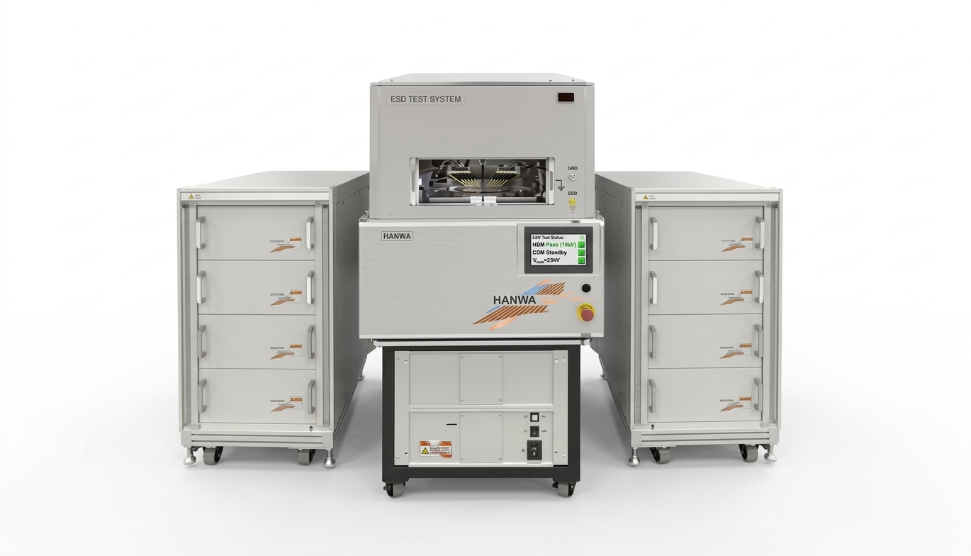
Hanwa ESD testers are known for their low-parasitic architecture and highly repeatable measurement behavior, making them particularly well-suited for advanced semiconductor devices and high-pin-count applications.
Their design emphasizes waveform stability and predictability — critical when qualifying sensitive components, troubleshooting failures, or comparing reliability results across multiple programs.
Modern Hanwa platforms also support multiple ESD and latch-up evaluation modes within a single system, allowing laboratories to consolidate test capability without added operational complexity.
Compliance with commonly used international ESD and latch-up test standards.
Highly repeatable stress waveforms for consistent pass/fail characterization.
Support for complex, high-pin-count devices without compromising signal integrity.
Stable pulse control to minimize variation across repeated test cycles.
Data consistency required for certification, audit, and customer reporting.
From package-level ESD to wafer-level, CDM, TLP, and latch-up — Hanwa consolidates test capability into a single, qualification-ready platform family.
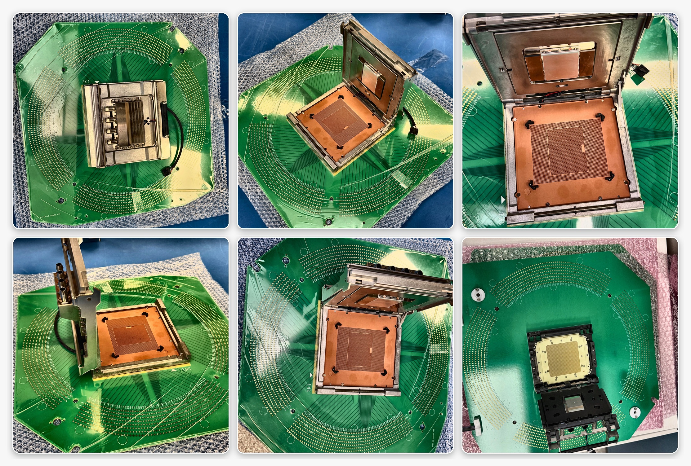
Non-relay GNC module supporting up to 2,048 pins. Low-parasitic architecture for high-precision detection on advanced devices.
Fully automated, integrated final-test system for production lines and research labs, with electrical, capacitance, and resistance test modes.
HBM & MM waveform testing at the wafer level. 0–±4kV charging (8kV option) with 1% ± 5V accuracy.
Charged Device Model testing conforming to JS-002, JEDEC, ESDA, and AEC specifications — the recommended model of leading semiconductor companies.
Transmission Line Pulse testing for investigating device protection circuits and correlating results with ESD failure analysis.
Tell us your device mix and test standards — we'll map the right Hanwa platform to your program.
You don't just need an ESD tester — you need a supportable reliability workflow. ASM-360 provides U.S.-based technical support, integration assistance, and sustainment services across the full operational lifecycle.
A Hanwa ESD tester is the backbone of a defensible, repeatable reliability strategy — supporting engineering decisions, customer commitments, and long-term product confidence. When validated and supported correctly, it becomes a trusted instrument for development, screening, and qualification, delivering repeatable results without unnecessary operational risk.
Tell us about your device mix, throughput needs, and test standards — ASM-360 will map the right Hanwa platform and support model for your lab.